PCBs PROTOTYPING

Printed Circuit Boards (PCBs) are at the heart of modern electronic devices, making rapid and reliable prototyping essential for innovation. Laser-based PCB prototyping enables the direct structuring of copper layers from standard Gerber files, allowing functional boards to be produced within hours rather than days or weeks. 

By eliminating masks, chemicals, and external fabrication steps, laser processing provides a clean, flexible, and highly controllable workflow. Fine features, accurate double-sided alignment, drilling, and board outlining can all be integrated into a single platform, accelerating design validation and reducing development cycles for electronics R&D, universities, and innovation labs.

Typical Features & Process Capabilities

KEY BENEFITS

Why LABCORE?

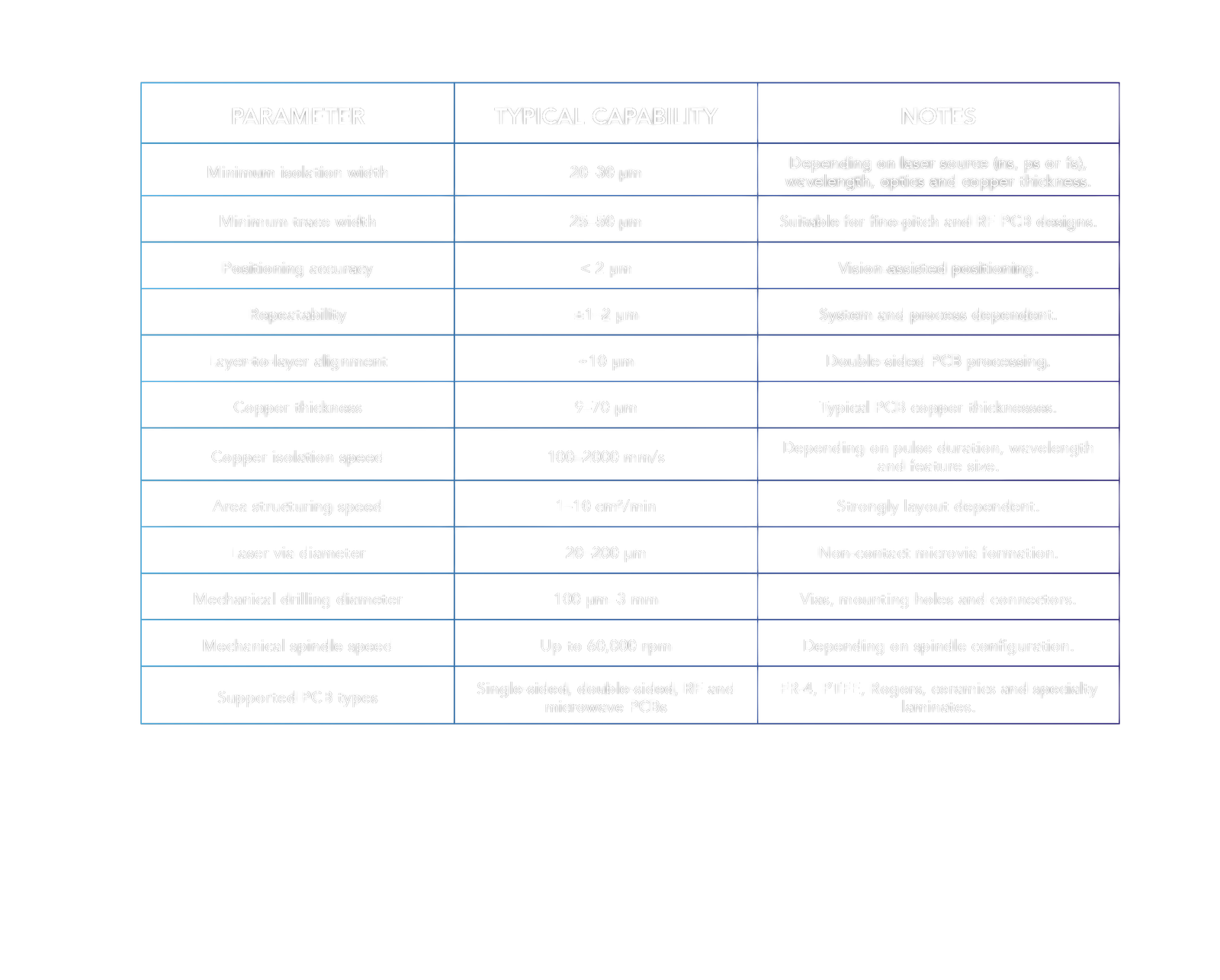
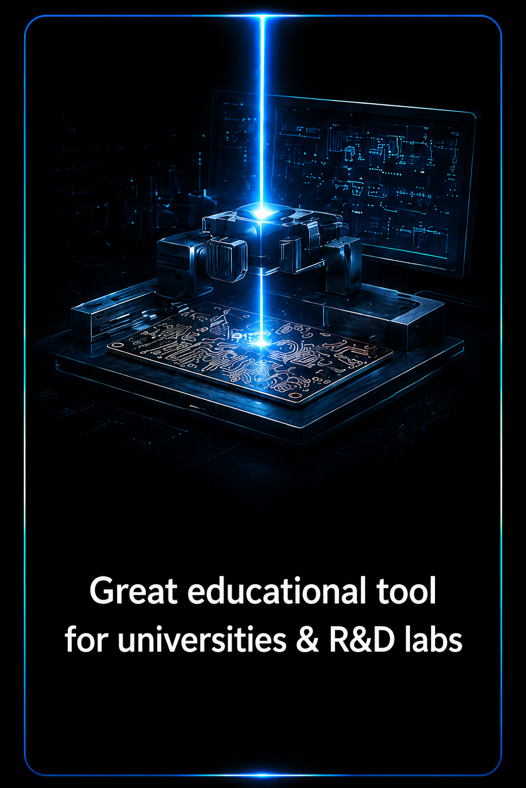
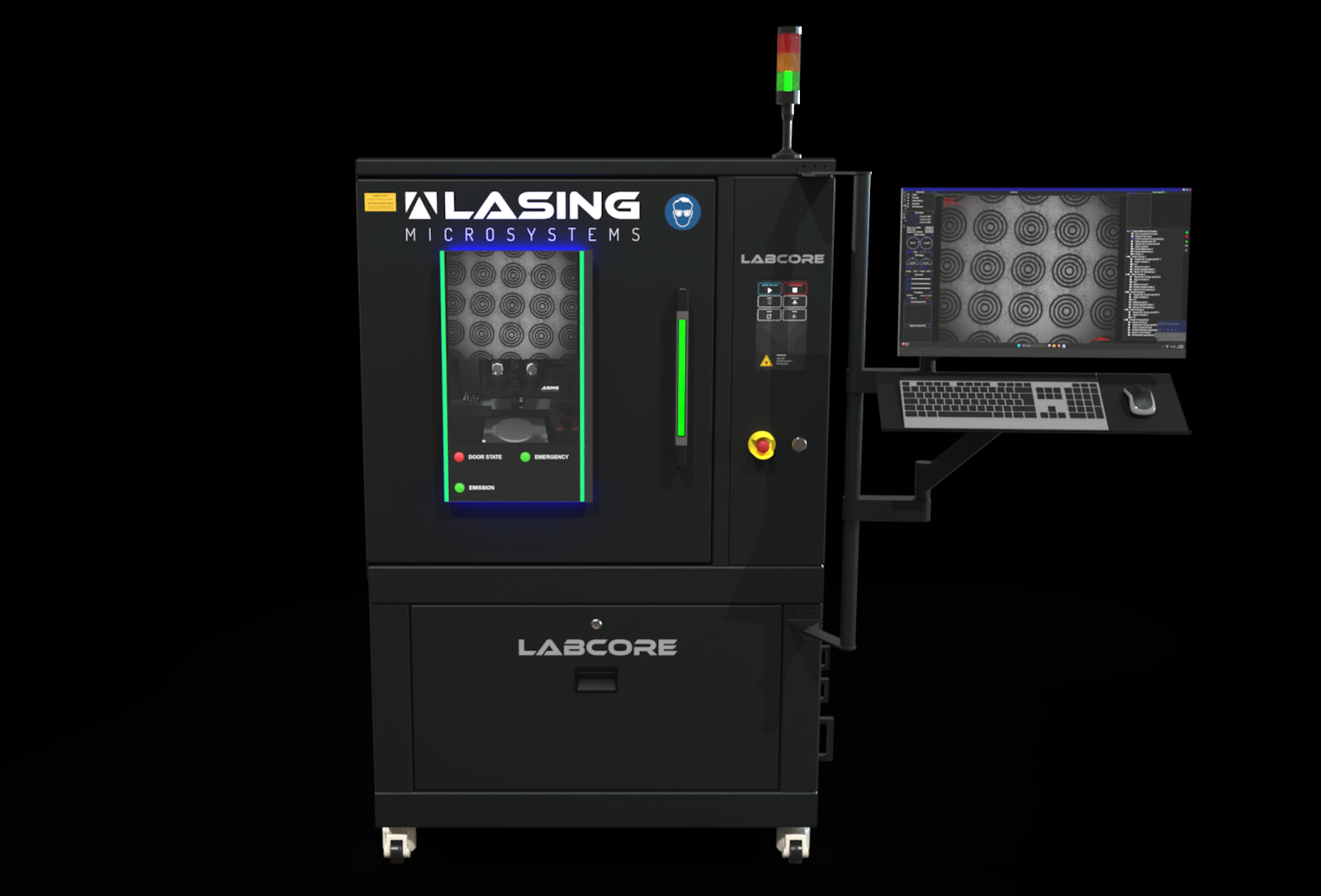
We have specialized our product LABCORE to cover the full PCB prototyping chain on a single but configurable system: laser ablation of copper layers, precise alignment for double-sided boards, optional mechanical drilling, and efficient debris extraction to keep processes clean and repeatable.

With dedicated PCB software (built on KiCAD-based engine) and advanced vision tools allows users to seamlessly import designs, flip boards for double-face layouts, and align layers with micron-level accuracy. 

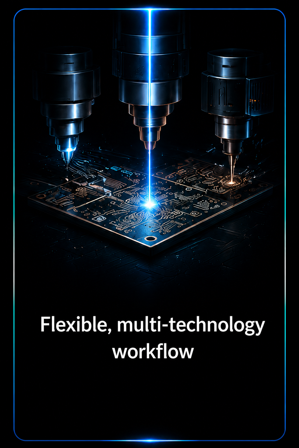
Thanks to its modular architecture, LABCORE supports multiple laser sources (fs, ps, or ns) and wavelengths (IR, green, UV), enabling users to balance resolution, speed, and material compatibility according to their needs.